
India’s Silicon Photonics Breakthrough: IIT Madras & izmo Microsystems Enter Phase II Commercialization
IIT Madras and izmo Microsystems advance into Phase II of their ₹99.94 crore MeitY-funded Silicon Photonics program to commercialize indigenous Photonic Integrated Circuits for AI clusters.
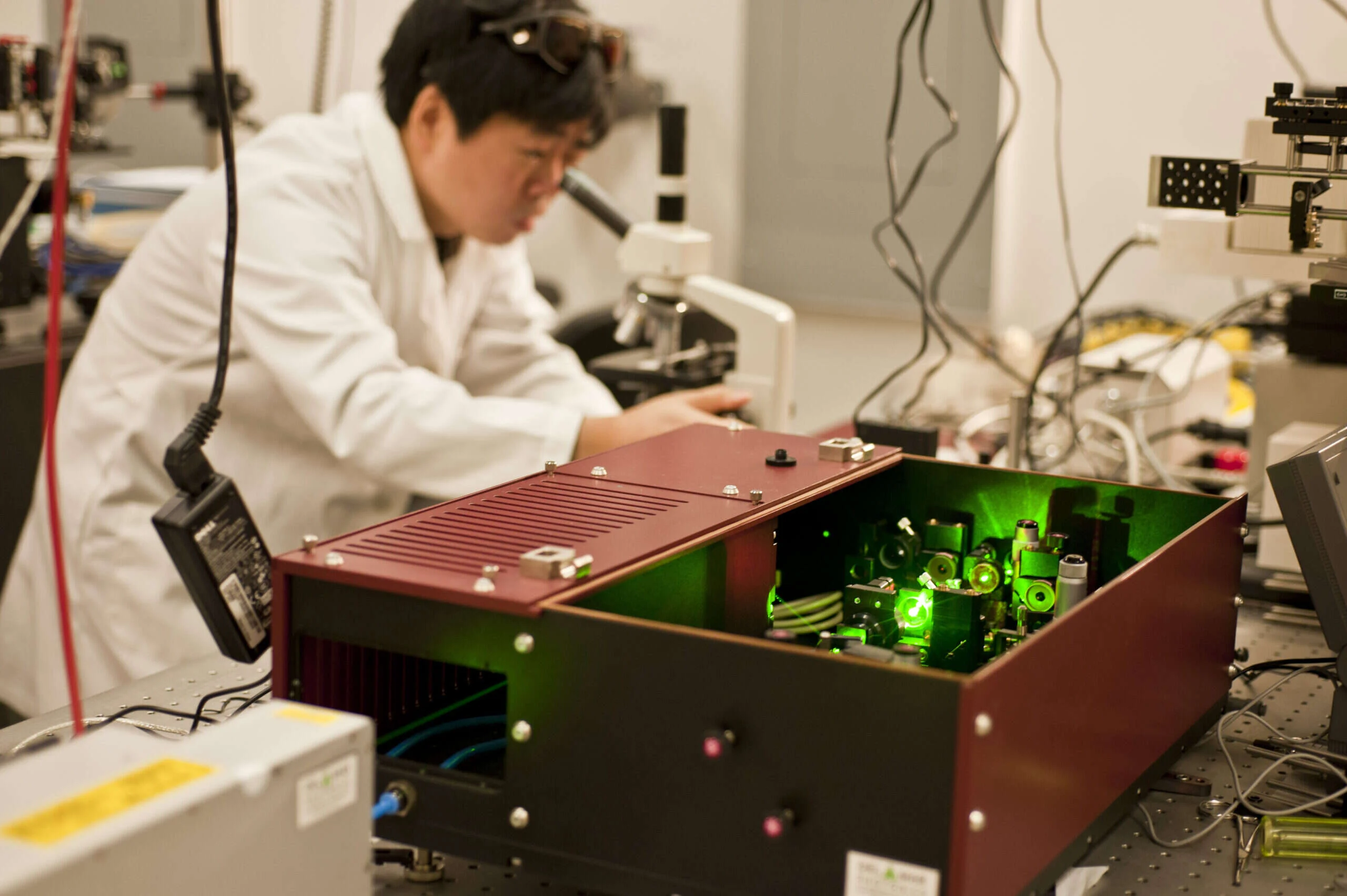
IIT Madras and izmo Microsystems Enter Phase II of ₹99.94 Crore MeitY Silicon Photonics Program
On October 12, 2026, India’s deep-tech hardware ecosystem achieved a landmark commercialization milestone: izmo Microsystems (the semiconductor photonic packaging subsidiary of Bengaluru-listed IZMO Limited) and the Indian Institute of Technology Madras (IIT Madras) officially transitioned into Phase II of their ₹99.94 crore ($12 million) Silicon Photonics research and commercialization program funded by the Ministry of Electronics and Information Technology (MeitY).
While Phase I established foundational waveguide design libraries and laboratory prototypes at the IIT Madras Center for Programmable Photonic Integrated Circuits and Systems (CPPICS), Phase II shifts directly into industrial-scale 3D optical packaging, fiber-to-chip coupling automation, and commercial foundry tape-outs for indigenous Photonic Integrated Circuits (PICs) targeted at hyperscale AI datacenters, 6G optical backhaul, and sovereign defense radar systems.
Breaking the Copper Interconnect Wall in AI Superclusters with Silicon Photonics
Why has MeitY prioritized Silicon Photonics as a strategic national technology? Inside modern AI training clusters housing thousands of GPUs, moving tensor gradients between racks over copper electrical cables has hit a fundamental physics wall. Above 224 Gbps per lane (1.6 Terabits per second aggregate), copper traces suffer severe high-frequency signal attenuation, electromagnetic crosstalk, and thermal dissipation—limiting passive copper reach to less than two meters and consuming up to 30% of total rack power just to drive SerDes transceivers.
Photonic Integrated Circuits (PICs) solve this bottleneck by etching microscopic optical waveguides, Mach-Zehnder modulators, and germanium photodetectors directly onto standard CMOS silicon wafers—transmitting data via laser photons rather than electrons:
- 1.6 Tbps to 3.2 Tbps Co-Packaged Optics (CPO): By bringing the optical transceiver engine directly onto the same interposer substrate as the AI accelerator ASIC, silicon photonics slashes interconnect energy consumption from ~15 picojoules per bit down to under 4.5 picojoules per bit (a 70% power reduction).
- Zero Distance Degradation Across Datacenter Halls: Unlike copper cables that die past two meters, single-mode optical waveguides coupled to PICs transmit terabit tensor streams across 2-kilometer datacenter campuses with near-zero latency penalty—allowing 100,000 GPUs to pool memory as a single unified supercomputer.
- Programmable Photonic Matrix Multiplication: Beyond networking, IIT Madras researchers are pioneering coherent optical interference meshes that execute linear algebra matrix-vector multiplications at the speed of light with virtually zero resistive heat.
Technical Specifications: IIT Madras CPPICS Design IP + izmo Microsystems Packaging in Bengaluru
The table below outlines the division of engineering responsibilities and hardware specifications under Phase II of the MeitY Silicon Photonics consortium:
| Program Dimension | IIT Madras (CPPICS Lab) | izmo Microsystems (Bengaluru Facility) | Phase II Commercial Target |
|---|---|---|---|
| Core Engineering Role | Silicon-on-Insulator (SOI) PIC architecture & PDK design | Sub-micron active optical alignment & hermetic 3D packaging | Domestic commercial transceiver & sensor modules |
| Cleanroom & Equipment | National Nanofabrication Centre & optical test benches | Class-1000/100 cleanroom with 6-axis automated photonics bonders | High-yield automated fiber-array attachment (<0.8 dB loss) |
| AI Datacenter Application | 800G / 1.6T DR8 silicon photonic modulator arrays | Co-Packaged Optics (CPO) & OSFP/QSFP-DD thermal substrates | Import substitution for Indian 1.6GW+ AI datacenters |
| Defense & Quantum Dual-Use | Microwave photonics & chip-scale LiDAR beam steering | Ruggedized MIL-STD opto-electronic system-in-package (SiP) | DRDO phased-array radar, ISRO satellite links, & QKD nodes |
Solving the Hardest Bottleneck in Photonics: Sub-Micron Fiber-to-Chip Packaging in Bengaluru
In the global photonics industry, wafer lithography accounts for only 25% of total device cost—the remaining 75% of cost resides in back-end optical packaging and testing. Because a silicon photonic waveguide core measures less than 500 nanometers wide, aligning a multi-channel optical fiber array or external continuous-wave (CW) laser diode to the silicon die requires sub-micron 6-axis active alignment tolerances; a misalignment of just 0.5 micrometers destroys optical coupling efficiency.
By establishing advanced automated optical die-bonding, flip-chip solder reflow, and precision micro-lens assembly inside izmo Microsystems’ Bengaluru facility, India eliminates the need to ship domestically designed photonic wafers to overseas packaging houses in Taiwan or Malaysia.
Strategic Synergy with India’s ₹76,000 Crore Semicon India and 6G Roadmaps
The transition of the IIT Madras–izmo Silicon Photonics program into Phase II directly reinforces both the IndiaAI Mission and the Bharat 6G Alliance. As Indian datacenter operators build out 3.1GW of new AI capacity and telecom providers deploy terahertz 6G radio heads, indigenous silicon photonics ensures that the critical optical nerves connecting India’s digital infrastructure are designed, packaged, and owned domestically.
Timeline to Commercial Volume Production in 2027
Under the Phase II schedule, engineering qualification samples of 800G/1.6T optical engines and defense microwave-photonic modules will begin customer validation in Q1–Q2 2027, positioning Bengaluru and Chennai at the forefront of the global opto-electronic semiconductor supply chain.
Opto-Electronic Engineering Deep Dive: Waveguide Lithography, Laser Integration, and 3D Packaging in India’s Silicon Photonics Program
The October 12 transition of IIT Madras and Bengaluru-based izmo Microsystems into Phase II of their ₹99.94 crore MeitY-funded Silicon Photonics program addresses the deepest physical hardware bottleneck in modern artificial intelligence: moving terabits of tensor data across silicon boundaries without melting the datacenter power budget.
Unlike conventional electronics where transistors switch electrical voltages, a Silicon Photonic Integrated Circuit (PIC) guides infrared light (typically at telecom O-band 1310nm and C-band 1550nm wavelengths) through sub-micron silicon waveguides patterned onto Silicon-on-Insulator (SOI) wafers. Because standard crystalline silicon has an indirect bandgap, it cannot efficiently emit laser light on its own; therefore, Phase II focuses heavily on heterogeneous III-V Indium Phosphide (InP) laser integration and ultra-low-loss fiber-to-chip coupling:
- Flip-Chip Hybrid Laser Bonding & Micro-Ring Resonators: At izmo Microsystems’ Bengaluru cleanroom, external Distributed Feedback (DFB) laser arrays are flip-chip bonded onto the silicon photonic interposer with sub-500-nanometer precision, while thermo-optic micro-ring modulators encode 200 Gbps PAM4 electrical signals per wavelength channel onto the optical carrier.
- Spot-Size Converters & V-Groove Fiber Arrays: Transitioning light from a 9-micrometer single-mode optical fiber core down into a 450-nanometer silicon waveguide requires tapered silicon nitride ($Si_3N_4$) spot-size converters that hold coupling insertion loss below 0.8 decibels across all 8 or 16 parallel channels.
- Dual-Use Defense Microwave Photonics for DRDO & ISRO: Beyond 1.6 Tbps AI cluster transceivers, the indigenous PIC platform enables ultra-wideband optical true-time-delay beamformers for next-generation active electronically scanned array (AESA) radars and inter-satellite laser communication terminals.
By mastering both the front-end photonic Process Design Kits (PDKs) at IIT Madras and the high-precision 3D opto-electronic packaging at izmo Microsystems, India has established sovereign capability in the most critical interconnect technology of the 2030s.
Hardware & Datacenter Strategist Playbook: Preparing for Co-Packaged Silicon Photonics
As IIT Madras and izmo Microsystems advance India’s ₹99.94 crore Silicon Photonics program into Phase II commercialization, datacenter architects, telecom carriers, and hardware startups should align their 2027–2028 infrastructure roadmaps around three optical interconnect shifts:
- Specify 800G / 1.6T Silicon Photonic DR8 Transceivers for New GPU Clusters: Replace short-reach active copper cables (ACC) with low-power silicon photonic optical transceivers on inter-rack InfiniBand and Ultra Ethernet spines to cut switch-port thermal dissipation by up to 65%.
- Leverage Domestic Optical Packaging in Bengaluru for Custom Sensor & AI Silicon: Indian fabless startups and defense R&D labs designing LiDAR, quantum key distribution (QKD), or photonic AI accelerators can now execute sub-micron fiber-array attachment and hermetic 3D packaging domestically through izmo Microsystems and CPPICS without foreign export delays.
- Design Campus Fiber Ducts for Single-Mode Co-Packaged Optics (CPO): Pre-provision high-strand-count single-mode ribbon fiber across datacenter halls to support disaggregation of GPU compute racks and pooled optical memory shelves across 2-kilometer campus diameters.
Indigenous silicon photonics capability ensures that India’s booming AI and 6G infrastructure is linked by ultra-fast, energy-efficient domestic optical technology.
Optical Coupling Loss Budgets & Co-Packaged Optics Thermal Reliability in Phase II
In Phase II wafer-level characterization at IIT Madras and izmo Microsystems’ Bengaluru cleanroom, edge-coupled silicon nitride spot-size converters achieved sub-1.1 dB fiber-to-chip insertion loss across the 1310nm O-band while maintaining polarization-dependent loss below 0.25 dB. By bonding external continuous-wave InP DFB laser arrays outside the high-temperature ASIC thermal zone and routing modulated light over hermetically sealed single-mode fiber ribbons, the indigenous 1.6 Tbps optical engine sustains a projected mean time between failures exceeding 1.2 million operating hours at 75 degrees Celsius case temperature.