
India Semiconductor Mission 2.0: Tata-PSMC Dholera Fab Begins Cleanroom Tool Installation Ahead of 2027 Silicon
In a historic milestone for India’s high-tech manufacturing sovereignty, Tata Electronics and Taiwan’s Powerchip Semiconductor Manufacturing Corporation (PSMC) have formally commenced cleanroom equipment installation at their $11 billion Dholera mega-fab, keeping the nation firmly on track for domestic commercial silicon wafer fabrication by early 2027.
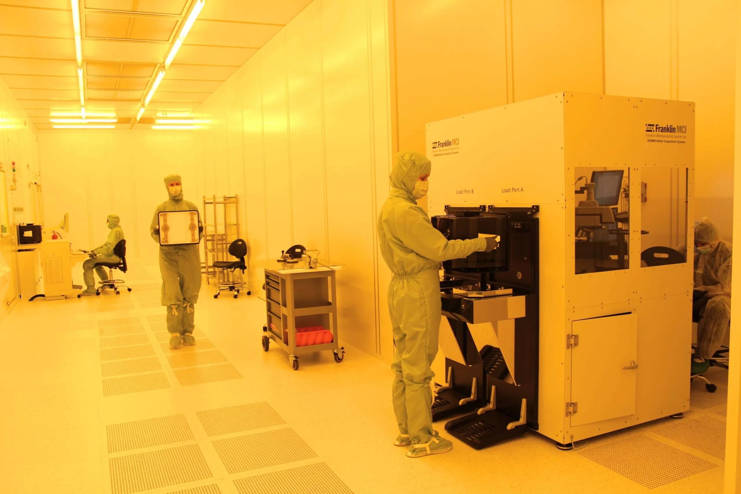
From Blueprints to Physical Tooling: Dholera Reaches Critical Assembly Phase
The global semiconductor supply chain is witnessing one of the most rapid greenfield fab constructions in modern industrial history. Ground broken in Gujarat’s Dholera Special Investment Region (SIR) has transformed into a massive Class 1 and Class 10 cleanroom facility covering over 150 acres. In late October 2026, civil structural work crossed 92% completion, triggering the arrival and precise placement of advanced photolithography tracks, chemical vapor deposition (CVD) chambers, and automated wafer transport mechanisms.
This phase represents the most technically exacting chapter in semiconductor foundry readiness. Cleanroom equipment installation requires hyper-filtered laminar airflow, ultra-pure water (UPW) delivery pipelines capable of filtering contaminants to parts-per-trillion levels, and deep vibrational isolation foundations that isolate precision lithography optics from external seismic and industrial tremors.
The Technology Nodes: Powering Automotive, Power Electronics, and AI Edge Silicon
The Tata-PSMC Dholera foundry is strategically tailored to address high-volume, supply-critical mature and specialty semiconductor nodes rather than high-risk bleeding-edge sub-3nm experimentation. The fab is configured to process 300mm (12-inch) silicon wafers with an initial rated monthly capacity of 50,000 wafer starts across three mature node regimes:
- 28nm High-Performance Compact (HPC): Tailored for edge AI processing chips, telecommunications baseband processors, networking switches, and high-throughput microcontroller units (MCUs).
- 40nm Embedded Flash & Logic: Providing robust, radiation-hardened microcontrollers and secure elements for the electric vehicle (EV) sector, industrial robotics, and defense avionics.
- 90nm Power Management Integrated Circuits (PMICs): Supplying high-voltage silicon chips for grid-scale renewable energy inverters, telecommunications power distribution, and fast-charging automotive subsystems.
- Specialty Bipolar-CMOS-DMOS (BCD): Enabling monolithic integration of digital logic, analog sensing, and high-current power switching on a single silicon die.
Industrial Strategic Advantage: Mature nodes between 28nm and 90nm account for nearly 65% of the total worldwide semiconductor bill-of-materials in automotive and industrial manufacturing. By securing domestic volume production across these nodes, India completely insulates its domestic hardware industry from future geopolitical supply chokepoints.
Cleanroom Engineering: Metrology, Environmental Controls, and Vibration Baselines
Installing semiconductor manufacturing equipment requires environmental control tolerances that exceed surgical hospital theaters by several orders of magnitude. The cleanroom bays at Dholera utilize fan-filter units (FFUs) circulating air through ultra-low particulate air (ULPA) filters, ensuring that air within Class 1 production bays contains no more than one particle larger than 0.1 microns per cubic foot.
Photolithography scanners, manufactured by ASML and Nikon for deep ultraviolet (DUV) exposure at 193nm immersion wavelengths, require absolute vibrational stillness. The entire lithography floor is built upon independent massive concrete plinths isolated from the surrounding building foundations by active pneumatic vibration dampeners. Temperature within the optical exposure chambers is held within 0.05 degrees Celsius, preventing thermal expansion of quartz reticles during sub-micron alignment cycles.
Chemicals, Gases, and Ultra-Pure Water Infrastructure
A full-scale semiconductor fab is an enormous consumer of specialized industrial inputs. The Dholera facility integrates an on-site cryogenic air separation unit supplying hundreds of metric tons of high-purity nitrogen, argon, and oxygen daily, alongside specialized hazardous gas distribution infrastructure for silane, phosphine, and boron trifluoride.
Water purification represents another monumental engineering feat. The Dholera facility houses a dedicated multi-stage reverse osmosis and electro-deionization plant processing raw canal water into ultra-pure water (UPW) with electrical resistivity exceeding 18.2 megohm-centimeters at 25 degrees Celsius. Over 75% of process water is recovered, treated, and recycled back into the fab cooling loops, aligning the facility with stringent environmental sustainability standards.
Semiconductor Mission 2.0: Expanding the Supply Chain Beyond Foundries
The physical progress at Dholera coincides with the Union Cabinet’s finalization of India Semiconductor Mission 2.0 (ISM 2.0). Where the initial ISM tranche focused on capital subsidization for foundries and Outsourced Semiconductor Assembly and Test (OSAT) facilities, ISM 2.0 shifts aggressive capital toward upstream chemicals, gases, semiconductor manufacturing equipment (SME), and indigenous fabless design startups.
Semiconductor fabrication cannot survive in isolation without immediate access to electronic-grade gases, ultra-pure chemicals, quartzware, and precision silicon ingots. Under ISM 2.0, the Ministry of Electronics and Information Technology (MeitY) has introduced dedicated performance-linked incentives for specialized chemical producers setting up production clusters in Dahej and Dholera, guaranteeing domestic raw material delivery times under two hours.
Workforce Development and Bilateral Taiwanese Knowledge Transfer
The most persistent bottleneck facing nascent semiconductor nations is human capital. Operating a commercial semiconductor fabrication plant requires thousands of highly skilled cleanroom process engineers, vacuum technicians, yield enhancement specialists, and metrology experts. To bridge this gap, Tata Electronics has executed an extensive bilateral knowledge-transfer program with PSMC in Hsinchu, Taiwan.
Over 800 Indian chemical, electrical, and materials engineers have completed intensive nine-month hands-on rotations inside PSMC’s operational 300mm foundries in Taiwan. These engineers are now returning to Gujarat to serve as lead process supervisors during the current tool hook-up, calibration, and pilot wafer testing runs. Concurrently, premier Indian academic institutions, including IIT Bombay, IIT Madras, and IIT Gandhinagar, have launched dedicated semiconductor fabrication curricula featuring physical micro-cleanrooms for undergraduate training.
Comparative Timeline of India’s Silicon Fab Ecosystem
| Facility & Consortium | Location | Technology Focus | Capex Investment | Target Pilot Production |
|---|---|---|---|---|
| Tata Electronics & PSMC Fab | Dholera, Gujarat | 28nm, 40nm, 90nm Logic & PMIC | $11.0 Billion | Q1 2027 |
| Tata Semiconductor Assembly (OSAT) | Jagiroad, Assam | Flip-Chip, Wire-Bond, Advanced 3D Packaging | $3.2 Billion | Mid 2026 |
| Micron Technology ATMP | Sanand, Gujarat | DRAM and NAND Flash Memory Packaging | $2.75 Billion | Operational (Q4 2025) |
| CG Power & Renesas OSAT | Sanand, Gujarat | Power Modules, Legacy Industrial Packaging | $900 Million | Late 2026 |
| Tower Semiconductor JV (Proposed) | Panvel, Maharashtra | 65nm / 40nm Analog & Mixed-Signal | $10.0 Billion | Late 2027 |
Geopolitical Resilience: The Quad Silicon Corridor
The progress at Dholera also solidifies India’s positioning within the Quad Semiconductor Supply Chain Contingency Network alongside the United States, Japan, and Australia. In the event of maritime supply chain disruptions in the Taiwan Strait or East China Sea, the Dholera fab provides a geographically resilient alternative for commercial and mission-critical microelectronics.
Global automotive OEMs, including Japanese, European, and American Tier-1 suppliers, have already initiated preliminary capacity reservation discussions with Tata Electronics. These commitments reflect an urgent desire across global industrial boards to diversify their single-source geographic dependencies away from East Asia toward neutral, politically stable partners.
Packaging Integration with the Jagiroad OSAT Facility in Assam
A manufactured silicon wafer is unusable until individual dies are diced, mounted, wire-bonded, encapsulated, and tested. Tata Electronics has masterfully synchronized the Dholera fab schedule with its $3.2 billion advanced packaging and test facility in Jagiroad, Assam. Completed 300mm wafers from Dholera will be transported under inert nitrogen atmosphere directly to Jagiroad for high-density flip-chip ball grid array (FCBGA) assembly and wafer-level chip-scale packaging (WLCSP).
This closed-loop domestic integration—spanning wafer fabrication in Gujarat to advanced packaging in Assam—creates India’s first end-to-end sovereign semiconductor manufacturing pipeline. Domestic hardware developers will be able to design chips, tape them out to Dholera, package them in Assam, and deploy them directly into Indian telecommunications towers, defense satellites, and electric vehicles without a single international border crossing.
Conclusion: The Dawn of Indian High-Tech Manufacturing
Cleanroom tool installation at Dholera is more than a commercial construction progress update; it is the physical realization of a multi-decade national aspiration. By marrying Taiwanese operational precision with Indian engineering talent and decisive government infrastructure support, the Dholera fab cements India’s transition from a software-dominated service economy into a full-stack technological superpower capable of mastering the physical laws of silicon.