
Daily AI News: TSMC 2nm Production Timeline, ASML High-NA EUV Orders & US Tech Subsidies
The executive daily AI intelligence briefing: TSMC confirms its 2nm N2 production schedule with Gate-All-Around nanosheets, ASML reports record High-NA EUV scanner shipments, and federal CHIPS Act disbursements hit key semiconductor milestones.
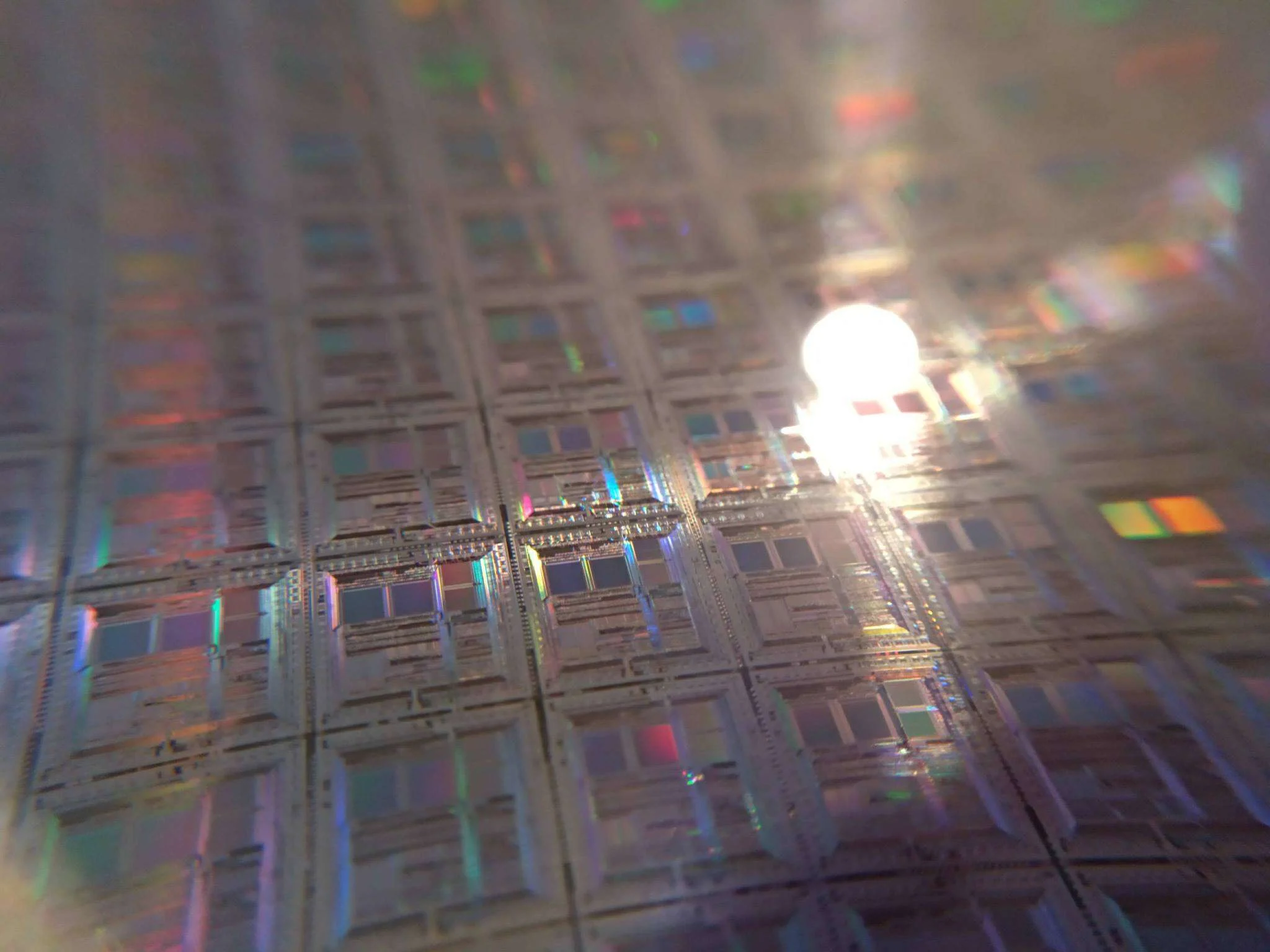
Photo: Wikimedia Commons / Creative Commons
The Silicon Frontline: Advanced Lithography & Transistor Physics
Welcome to today’s executive artificial intelligence dispatch. While high-level industry discourse frequently fixates on algorithmic architectures, model parameter scales, and transformer fine-tuning recipes, the ultimate pacing factor of the global AI revolution remains fundamentally tethered to atomic-scale manufacturing. Every frontier model release—from reasoning engines to multi-agent vision swarms—is constrained by the availability of high-density silicon fabricated within cleanrooms in Taiwan, Arizona, and Oregon.
Today, three monumental developments across the semiconductor supply chain have converged: Taiwan Semiconductor Manufacturing Company (TSMC) confirmed its commercial mass production schedule for its landmark 2nm (N2) node; Dutch lithography monopoly ASML released operational shipment disclosures regarding its next-generation High-NA EUV (Twinscan EXE) scanners; and the United States Department of Commerce finalized major capital milestones under the CHIPS and Science Act.
1. TSMC N2 Node: The Transition to Gate-All-Around (GAA) Nanosheets
Speaking at an executive investor symposium in Hsinchu, TSMC executive leadership officially reaffirmed that its next-generation 2nm N2 process node remains precisely on track for commercial volume ramp in late 2026:
- The End of the FinFET Era: After more than a decade of relying on Fin Field-Effect Transistors (FinFETs), TSMC is transitioning to Gate-All-Around (GAA) nanosheet transistor architectures. By encasing the conduction channel completely with the gate electrode on all four sides, GAA nanosheets drastically reduce quantum leakage currents and deliver unprecedented electrical control at atomic dimensions.
- Performance & Efficiency Gains: At identical power consumption profiles, TSMC’s N2 node delivers a 10% to 15% increase in operational clock frequencies compared to the current N3E node. Alternatively, at matched compute frequencies, N2 slashes power consumption by 25% to 30%, while increasing transistor logic density by more than 15%.
- Backside Power Delivery (A16 Architecture): TSMC confirmed that its subsequent iteration, the A16 node (scheduled for late 2027), will integrate backside power delivery networks (Super Power Rail), decoupling power rails from signal interconnects to boost compute density in next-generation AI accelerators.
- The Customer Queue: Industry procurement reports indicate that Apple, NVIDIA, and AMD have already fully booked TSMC’s initial N2 capacity allocations through mid-2027, securing the physical silicon required for next-generation frontier accelerators and mobile neural engines.
2. ASML High-NA EUV: Sub-Atomic Precision at Commercial Scale
In Veldhoven, Netherlands, ASML disclosed quarterly operational benchmarks confirming the successful shipment and customer cleanroom assembly of multiple Twinscan EXE:5000 High-NA EUV lithography systems:
- The Physics of High-NA: Moving from standard EUV’s 0.33 Numerical Aperture to High-NA’s 0.55 NA anamorphic lens system allows chipmakers to print circuit features down to 8 nanometers in a single exposure. This eliminates the need for expensive, defect-prone multi-patterning techniques required on standard 0.33 NA systems.
- Price & Logistics Reality: Each High-NA scanner represents an investment exceeding $380 million (approx. €350 million), weighing over 150 metric tons and requiring three Boeing 747 cargo aircraft to transport. Intel, TSMC, and Samsung remain the sole semiconductor fabrication companies possessing the capital envelope required to integrate these machines.
3. CHIPS Act Milestones: Federal Capital Reaches Fabrication Cleanrooms
In Washington, D.C., the Department of Commerce announced that federal grant disbursements under the $52.7 billion CHIPS and Science Act have officially transitioned from preliminary non-binding memoranda of terms into binding financial capital transfers:
| Semiconductor Leader | Binding Grant Total | Target Facilities | Operational Timeline |
|---|---|---|---|
| TSMC Arizona | $6.6 Billion Direct Funding | Fab 21 (Phase 1: 4nm; Phase 2: 3nm/2nm) | Volume commercial production late 2025 – 2026 |
| Intel Corporation | $8.5 Billion Direct Funding | Ohio One Megasite & Oregon R&D Hubs | Intel 18A volume ramp scheduled 2025–2026 |
| Samsung Electronics | $6.4 Billion Direct Funding | Taylor, Texas Advanced Foundry & Packaging | Advanced 4nm / 2nm foundry production 2026 |
| Micron Technology | $6.1 Billion Direct Funding | New York & Idaho Leading-Edge HBM Memory Fabs | High-Bandwidth Memory (HBM4) domestic supply |
What This Means for the Global Enterprise AI Horizon
The technological implications of today’s semiconductor announcements reverberate throughout the entire enterprise software ecosystem:
- The Compute Cost Deflation Curve Continues: The commercial realization of 2nm GAA nanosheets ensures that the dollar-per-FLOP compute deflation curve will sustain momentum through the late 2020s, enabling frontier laboratories to train 10-trillion-parameter reasoning systems without hitting thermal saturation walls.
- The Critical Role of Advanced Packaging (CoWoS): Transistor shrinking alone is no longer sufficient; the primary operational bottleneck in AI silicon remains advanced packaging (TSMC’s Chip-on-Wafer-on-Substrate). Capacity expansions in Taiwan and the US will determine whether hyperscaler order backlogs clear in 2026.
- Geopolitical Supply Chain Resilience: With leading-edge foundries advancing across Phoenix, Arizona and Dresden, Germany alongside Taiwan, global enterprises can anticipate greater geographic diversification and reduced single-point-of-failure vulnerability in global AI silicon supplies.
The Transistor Packaging Revolution: CoWoS, SoIC & Silicon Photonics
While TSMC’s 2nm N2 node represents the pinnacle of atomic-scale transistor lithography, modern artificial intelligence accelerators have grown far too large to be manufactured on a single monolithic silicon die. The physical reticle limit of standard lithography scanners (approximately 858 square millimeters) caps the maximum physical area of a single chip.
To continue scaling compute performance, the semiconductor industry has shifted definitively toward Advanced Multi-Die Packaging and Chiplet Architectures:
- TSMC CoWoS (Chip-on-Wafer-on-Substrate): The foundational packaging technology enabling modern AI accelerators (such as NVIDIA’s B200 and AMD’s MI300X). By bonding multiple compute logic dies side-by-side with High-Bandwidth Memory (HBM3e and HBM4) stacks on an ultra-dense silicon interposer, CoWoS enables terabytes per second of inter-chip memory bandwidth.
- TSMC SoIC (System-on-Integrated-Chips): The next evolutionary step in 3D vertical stacking. SoIC bonds logic dies directly on top of memory or base dies with sub-micron pitch accuracy without utilizing microbumps, reducing signal transmission latency and power loss by over 80%.
- Co-Packaged Optics & Silicon Photonics: As copper electrical interconnects hit fundamental physical resistance limits at multi-gigabit speeds, TSMC and partners are industrializing Silicon Photonics. By integrating optical laser transceivers directly into the chiplet package, datacenters can interconnect thousands of GPU clusters using light, slashing networking power consumption by up to 70%.
The Strategic Takeaway for Enterprise Technology Leaders
The technological momentum across TSMC, ASML, and federal CHIPS Act fabrication hubs delivers a decisive message to enterprise technology executives: the physical infrastructure powering artificial intelligence is undergoing the most capital-intensive expansion in industrial history. Computing capacity will not hit a hardware wall; rather, it will continue to accelerate, lowering unit inference costs and making pervasive multi-agent enterprise automation economically inevitable.
Primary Citations & Industry Documentation
- Taiwan Semiconductor Manufacturing Company (TSMC). (October 2026). Quarterly Technology Symposium: N2 GAA Nanosheet Progress & A16 Roadmap. Official Company Disclosures, Hsinchu, Taiwan.
- ASML Holding N.V. (2026). High-NA EUV Technology Milestones: Twinscan EXE:5000 Industrialization Report. Veldhoven, Netherlands.
- United States Department of Commerce. (2026). CHIPS Program Office: Finalized Binding Capital Agreements and Fabrication Milestones. National Institute of Standards and Technology (NIST), Washington, D.C.
- Semiconductor Industry Association (SIA). (2026). State of the Global Semiconductor Industry: 2026 Mid-Year Strategic Review. Washington, D.C.
Navigating Enterprise Compute Architecture or AI Silicon Strategy?
ABATA AI engineers custom inference topologies and sovereign governance pipelines around Daily AI News: TSMC 2nm Production Timeline, ASML High-NA EUV Orders & US Tech Subsidies (daily-ai-news-tsmc-2nm-pro). Schedule a technical architecture review with our engineering team.