
Tata Electronics & PSMC Dholera Semiconductor Fab: Cleanroom Structural Readiness & 28nm Pilot Line Roadmap
India’s semiconductor manufacturing ambitions crossed a historic physical threshold today as the Tata-PSMC joint venture achieved cleanroom certification at Dholera, Gujarat.
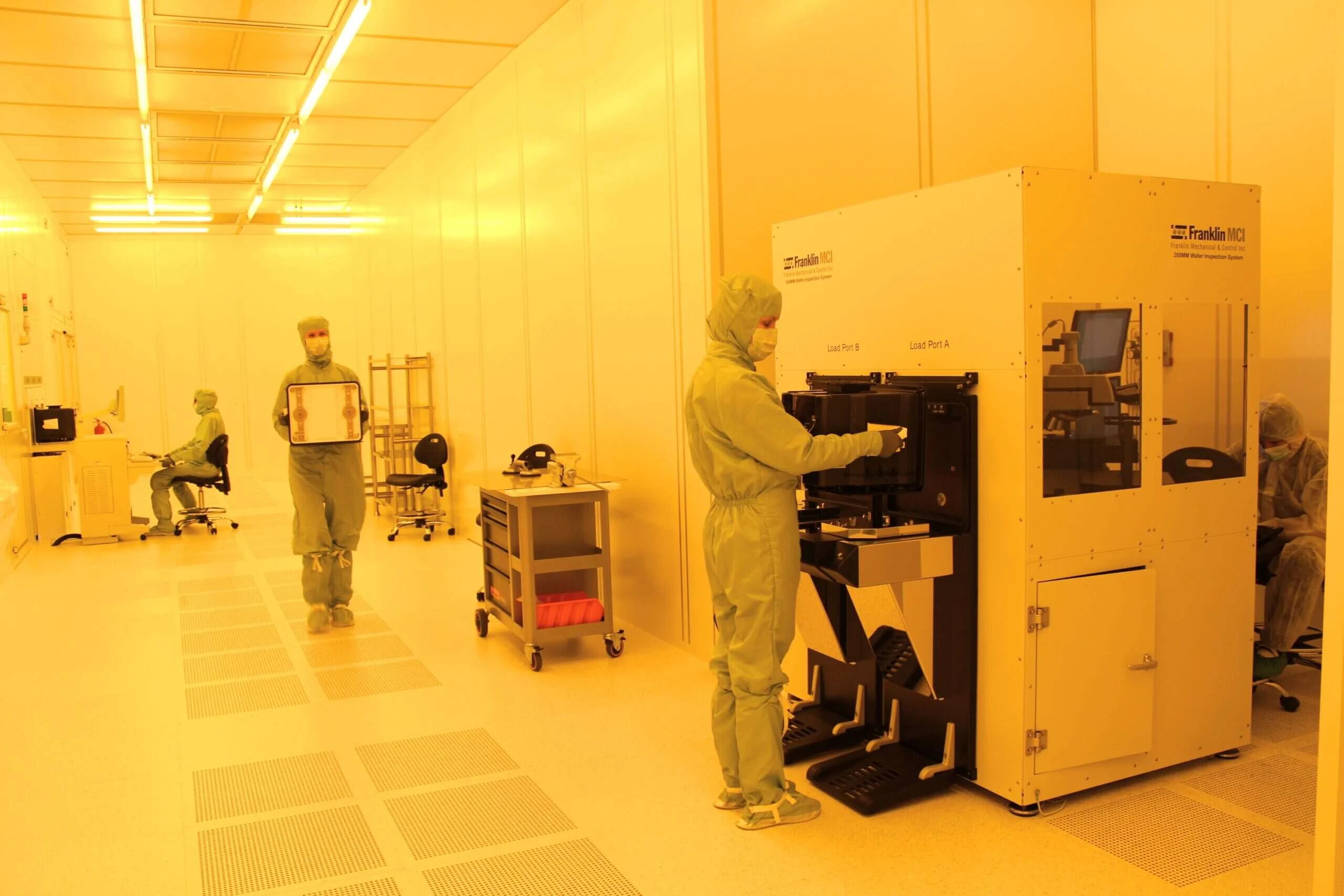
Physical Realization of India’s Silicon Ambitions
India’s multi-decade quest to establish commercial silicon wafer fabrication entered its decisive physical phase today. Tata Electronics Private Limited (TEPL), in strategic technical partnership with Taiwan’s Powerchip Semiconductor Manufacturing Corporation (PSMC), officially announced the structural completion and initial cleanroom certification of the $11 Billion (₹91,000 crore) commercial semiconductor fab located in the Dholera Special Investment Region (SIR), Gujarat.
Supported by the central government’s India Semiconductor Mission (ISM) with a 50% fiscal capital expenditure subsidy, the Dholera facility represents India’s first commercial, high-volume chip manufacturing fab, engineered to produce up to 50,000 wafer starts per month (WSPM).
1. Cleanroom Validation & Tool Hook-Up Schedule
The facility features over 100,000 square feet of certified Class 10 and Class 100 cleanroom manufacturing space. Structural isolation pads engineered to eliminate seismic and vibrational interference from nearby transit corridors have been validated to sub-micron standards.
With structural completion accomplished on schedule, Tata Electronics has commenced the installation of precision fab equipment, including Deep Ultraviolet (DUV) lithography scanners, atomic layer deposition (ALD) chambers, chemical-mechanical planarization (CMP) tools, and automated overhead wafer transport (OHT) tracks.
2. Node Roadmap: 28nm, 40nm, and Power Management ICs
While cutting-edge 2nm and 3nm nodes capture consumer headlines, the economic backbone of global industrial, automotive, and telecommunications electronics relies on mature and legacy nodes:
- 28nm High-Performance Compact (HPC+): Target production for baseband communication chips, IoT microcontrollers, display driver ICs, and edge AI inferencing silicon.
- 40nm / 55nm Automotive & Industrial Logic: Certified automotive-grade electronic control units (ECUs), motor control processors for electric vehicles (EVs), and smart grid power sensors.
- Power Management & BCD (Bipolar-CMOS-DMOS): High-voltage silicon switches, battery management chips, and telecom power management modules for 5G/6G base stations.
Dholera Fab Project Specifications & Economic Milestones
| Metric / Parameter | Dholera Mega Fab Specification | Strategic Industrial Impact |
|---|---|---|
| Total Capital Outlay | $11 Billion (₹91,000 Crore) | Largest private deep-tech investment in Indian history |
| Wafer Capacity | 50,000 WSPM (300mm / 12-inch) | Supplies ~20% of domestic automotive & industrial demand |
| Technology Partner | PSMC (Taiwan) | Direct technology transfer & operational IP licensing |
| Primary Technology Nodes | 28nm, 40nm, 55nm, 90nm | Addresses high-reliability industrial & automotive sectors |
| Pilot Line Wafer Run | Late 2026 / Early 2027 | Domestic test wafer qualification across key OEMs |
Catalyzing the Domestic Electronics Ecosystem
The operationalization of the Dholera cleanroom creates immediate secondary industrial ripple effects. Upstream suppliers—including ultra-pure chemical manufacturers, electronic gas providers (nitrogen, argon, silane), and precision test equipment vendors—have begun establishing localized facilities within the Dholera SIR. Coupled with Tata’s semiconductor assembly and test (OSAT) facility in Jagiroad, Assam, India is assembling a fully integrated, resilient sovereign chip supply chain.